Electronics and Semiconductor Manufacturing Robotics
Semiconductor wafer handling in vacuum cluster tools, high-speed SMT assembly, wire bonding, and automated optical inspection.
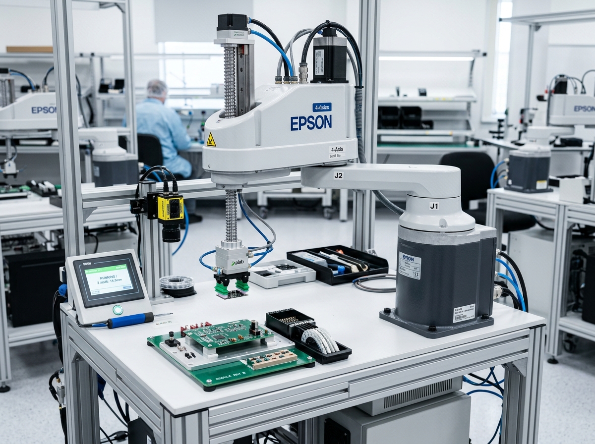
Placement Accuracy
Sub-pixel telecentric vision calibration
Takt Output Rate
Continuous high-speed SMT assembly velocity
Cleanroom Standard
Particle-free sealed grease & stainless seals
Defect Interception
Deep CNN sub-pixel solder bridging classification
Robotic Applications in Electronics and Semiconductor Manufacturing
Turnkey robotic workcells, kinematic metrics, and operational architectures deployed across modern electronics and semiconductor manufacturing manufacturing plants.
High-Speed SCARA PCB Component Placement
Direct-drive SCARA robots placing micro-fasteners, shielded connectors, and delicate 01005 chips at high cycle frequencies.
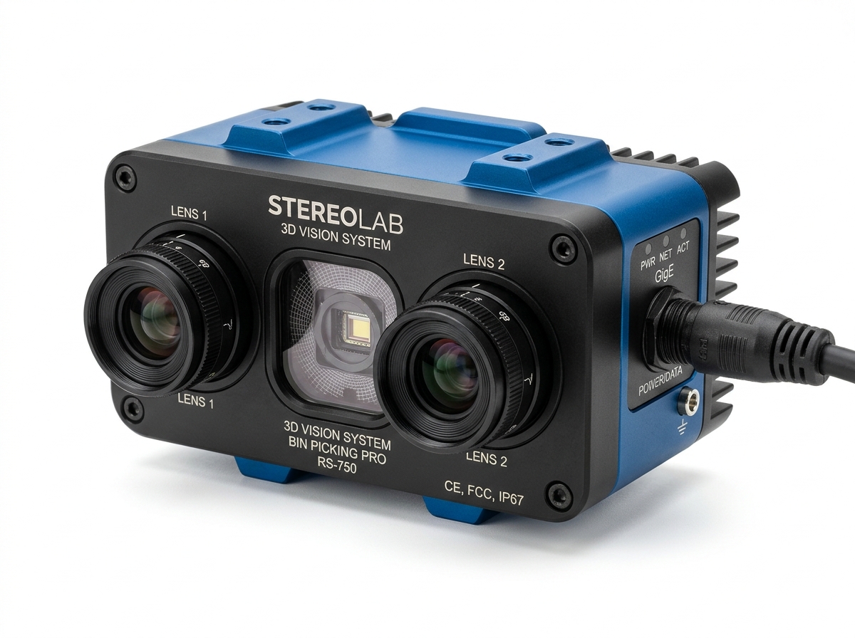
Automated Wafer FOUP & Pod Transfer Manipulators
Precision dual-arm Bernoulli and vacuum end-effectors transferring 300mm silicon wafers between cassette pods and lithography stages.
Select Your Electronics and Semiconductor Manufacturing Automation Requirement
Toggle between core automation processes to inspect matching kinematic models, payload capacities, cycle times, and directly download engineering CAD files.
INDUS-SCARA-S12
Engineered for high-frequency micro-pick and place in semiconductor packaging and consumer electronics SMT lines.
Electronics and Semiconductor Manufacturing Automation Use Cases
Every production task has specific mechanical shock profiles, positioning tolerances, sensing architectures, and functional safety constraints. Explore detailed engineering breakdowns for each verified operation.
Cluster Tool High-Vacuum (10^-8 Pa) Wafer Transfer Robot
Standard mechanical gearing sheds particles and outgasses lubricants in vacuum, contaminating multi-million dollar wafer batches.
Dual-arm SCARA/frog-leg vacuum robot with ceramic end-effector blades and magnetic fluid feedthroughs.
Transfer of 300mm silicon wafers between vacuum deposition and etching process chambers in ultra-high vacuum (<10^-8 Pa).
EUV Photolithography Reticle Mask Positioning Stage
Extreme ultraviolet lithography requires sub-nanometer position holding while scanning masks under extreme acceleration (>30G).
Magnetically levitated (maglev) 6-DoF stage driven by ironless planar linear motors.
Continuous 6-DoF planar scanning of photomask reticles in high-vacuum EUV environment.
Ultra-High Speed (100,000 CPH) SMT Component Placement
Placing microscopic 0201 and 01005 metric passive components requires sub-15ms pick-orient-place cycles without mechanical bounce.
Multi-head rotary gantry robot equipped with 16 independent vacuum nozzles and on-the-fly vision cameras.
Surface mount placement of micro-electronic passives onto printed circuit boards moving on conveyor line.
High-Speed Thermosonic Semiconductor Wire Bonding
Connecting 15-micron gold/copper bonding wires between microchip die pads and leadframes at 18 wires per second.
High-dynamic X-Y-Z Cartesian stage driven by linear voice-coil motors and air-bearing guides.
Micro-welding of electrical interconnects on heated semiconductor leadframe (200°C) with ultrasonic transducer.
Automated Optical Inspection (AOI) for Unpatterned Wafer Defects
Detecting sub-20nm particulate and crystal defect pits on bare 300mm silicon wafers without adding inspection artifacts.
Direct-Drive Rotary (DDR) air-bearing vacuum chuck coupled to continuous linear scanning axis.
High-speed continuous helical spiral scanning of spinning wafer under darkfield laser illumination.
High-Precision Flip-Chip Micro-Die Bonding
Aligning thousands of microscopic micro-bumps on advanced packaging chiplets (HBM, GPU) with sub-micron coplanarity.
High-accuracy dual-gantry Cartesian die bonder with heated bonding collet (up to 400°C).
Picking inverted silicon dies from dicing tape and thermal compression bonding onto interposer substrates.
Cleanroom AMR FOUP Carrier Transfer in 300mm Fabs
Overhead Hoist Transport (OHT) track bottlenecks during fab expansion require flexible floor-level wafer cassette transfer.
Omnidirectional cleanroom AMR with integrated vibration-isolated collaborative 6-axis loading arm.
Autonomous transport of 300mm Front Opening Unified Pods (FOUPs, 9 kg) between stockers and lithography tools in fab cleanroom.
Selective Conformal Coating of Automotive ECU Boards
Coating must precisely coat fine-pitch IC pins while keeping connectors and test points 100% free of insulating lacquer.
Benchtop 4-axis Cartesian robot with tilt-swivel spray dispensing valve and UV curing module.
4-axis robotic dispensing of acrylic or silicone conformal coating lacquer over complex populated circuit boards.
Automated Silicon Wafer Dicing Saw Robotic Tending
Ultra-thin diced wafers (down to 30 microns) mounted on dicing film are fragile and can curl or tear during automated handling.
Cleanroom SCARA robot equipped with non-contact Bernoulli vacuum gripper.
Loading and unloading 300mm wafer dicing frames into high-speed diamond dicing saw with high-purity DI water spray.
Automated 3D Computed Tomography (CT) BGA Solder Void Inspection
Hidden solder voids beneath Ball Grid Array (BGA) and QFN chips cannot be inspected optically.
High-precision 5-axis granite-base robotic positioning manipulator inside lead-shielded cabinet.
Precision multi-angle X-ray projection of high-reliability aerospace PCBAs with automated 3D volume reconstruction.
High-Speed Flying Probe In-Circuit PCBA Electrical Tester
Bed-of-nails test fixtures cost thousands per revision; prototyping requires agile fixtureless testing of high-density SMT boards.
Dual-sided 8-axis linear motor gantry with micro voice-coil Z-axis needle actuators.
Contacting microscopic SMT test pads (100 µm pitch) with 8 high-speed independent moving needle probes.
High-Speed Diced Wafer Die-to-Tape Sort & Pack
Sorting good dies from defective ink-dotted dies on stretched wafer film at speeds over 12 dies per second.
Direct-drive dual-arm rotary turret picker synchronized with carrier tape indexer.
Ejector pin pushes die from underneath wafer film; robotic collet picks die and places into embossed carrier tape pocket.
Manufacturing Challenges & Robotic Solutions
Comparing conventional production bottlenecks against deterministic multi-axis robotic automation.
Electronics and Semiconductor Manufacturing Automation Hurdles
Demanding environmental conditions, high-speed cycle times, and precision limits dictate deterministic robotics.
- ISO Class 1 airborne particle cleanliness limits (<10 particles per m³ ≥0.1 µm)
- High vacuum operating environments (10^-7 Torr) causing standard grease outgassing
- Thermal settling oscillations degrading micro-positioning takt times
- Electrostatic discharge (ESD) risks that can instantly destroy sub-micron silicon gates
Robotic Automation Potential
High-stiffness mechanical transmission, multi-axis sensory feedback, and real-time motion control.
- Direct-drive ironless linear motors providing zero-cogging sub-micron scanning
- Dry-lubricated MoS2 coated strain-wave reducers for vacuum cluster tool end effectors
- Active piezoceramic vibration cancellation for high-resolution optical inspection stages
Accelerate Electronics and Semiconductor Manufacturing Automation
Access our specialized kinematics sizing tools, discuss payload vs cycle takt trade-offs, and receive 3D CAD space-claim models verified for this manufacturing discipline.
Connected Ecosystem
Other Manufacturing Sectors
Related Industrial Sectors
- Automotive
High-precision robotics meeting the extreme uptime and sub-millimeter tolerances of modern EV & automotive production.
- Electronics
Sub-micron repeatability and cleanroom-compliant automation for high-density electronic assemblies.
- Manufacturing
Rugged robotic automation engineered for high-uptime machine tending and harsh factory environments.